Please read the blog start first. This blog explains the 'common mode feedback' aspect in the circuit. A simple BJT breadboard circuit is build and some measurements are taken. The 'common mode feedback' makes the output floating X3 X4 and creates an 'anode coupled' amp differential characteristic for Q3 Q4.
the Start Blog please read this first!
To interconnection of katodengekoppeltem - understand and anodengekoppeltem differential amplifier, I made once the following experimental circuit with bipolar transistors :

Like that you can easily keep track of how and check. With the below given values one obtains a gain of 20dB. The operating voltage VCC = 24VDC allows line level at the outputs X3 and X4.
Resistor
R01 = R02 = 2K2Ω
2K2Ω
R03 = R04 = 1MW
6K8Ω
R05 = R06 = 1MW
820Ω R07 = 820Ω
R08 = R09 = 100ppm 100ppm
R10 = R11 = 200Ω 200Ω
R12 3K9Ω
= R13 = R14 = 100ppm 100ppm
R15 = R16 = 100ppm
2K2Ω
R17 = R18 = 100ppm 2K2Ω
R19 = 4K7Ω
Capacitors: C1 = 47uF 63VDC
positive terminal to Vcc
C2 = 1μF 63VDC negative pole connected to X1
C3 = 1μF 63VDC negative to X2
C4 = 1μF 63VDC positive pole at Q1
C5 = 1μF 63VDC positive at Q2
C6 = 100uF 25VDC negative to GND
C7 = 47uF 16VDC negative at X3
C8 = 47uF 16VDC negative on X4
C9 = 220μF 10VDC negative to GND
diodes:
D1 = 1N4148
D2 = 1N4148
transistors:
Q1 = BC547C
Q2 = BC547C
Q3 = BC547C
Q4 = BC547C
Short functional description of the components in detail:
Resistor
R1, R2 _Arbeitswiderstände for the difference amplifier transistors Q1, Q2.
R10, R11 _Stromgegenkopplungswiderstände for the transistors Q1, Q2. By their resistance to the working relationship resistors the gain rate, here is 20dB festegelgt. Hold the working slope of Q3, Q4 constant.
R16, R17 _Arbeitswiderstände for the difference amplifier transistors Q3 Q4.
R3, R5, R15, R19 _laden on the coupling capacitors and pull the connectors X1, X2, X3, X4 moderately high signal to GND.
R4, R12, R19 _teilen the operating voltage Vcc voltages in the operating point of the differential amplifier.
R8, R9 _Entkoppeln comparatively small signal, the bases of the DC voltage on C6. R13, 14 _Entkoppeln comparatively small signal, the bases of the DC at C9.
R6, R7 _Überstrom and vibration protection resistors to the bases of Q1, Q2.
Capacitors: C1
_Betriebsspannungsblock
C2, C3, C7, C8 _Koppelkondensatoren
C6 _Referenzspannungsblock
C9 _Referenzspannungsblock
C4 _Koppelkondensator combines moderately small signal collector of Q1 with a base of Q3.
C5 _Koppelkondensator combines moderately small signal collector of Q2 base of Q4.
diodes:
D1, D2 _verhindert the Zenern the base-emitter diode of Q1, Q2.
transistors:
Q1, Q2 _This differential amplifier pair is defined as follows in analogy to the differential amplifier katodengekoppelten in the text.
Q3, Q4 _This differential amplifier pair is defined as follows in analogy to anode coupled differential amplifier in the text.
A few basic, general observations on the differential amplifier.
A differential amplifier is characterized in that its differential gain is greater than its sum gain. Ideally, there will only differential gain. This is achieved by coupling two differential amplifier branches. The sum signal may, ideally, cause any change in current in the differential amplifier branches can. This requires, if the difference is not complementary amplifier paths are built next to the two tube or transistor stages yet, any kind , "Power Supply". This is the power of willing in accordance to the two levels of control, distributed. Small-signal standard depends on the symmetry of the output voltage to GND by the symmetry of the load resistors, but not on whether electrically equivalent transistors or tubes in the two branches are used. The only plays a role when the real "current source" too low internal resistance gets.
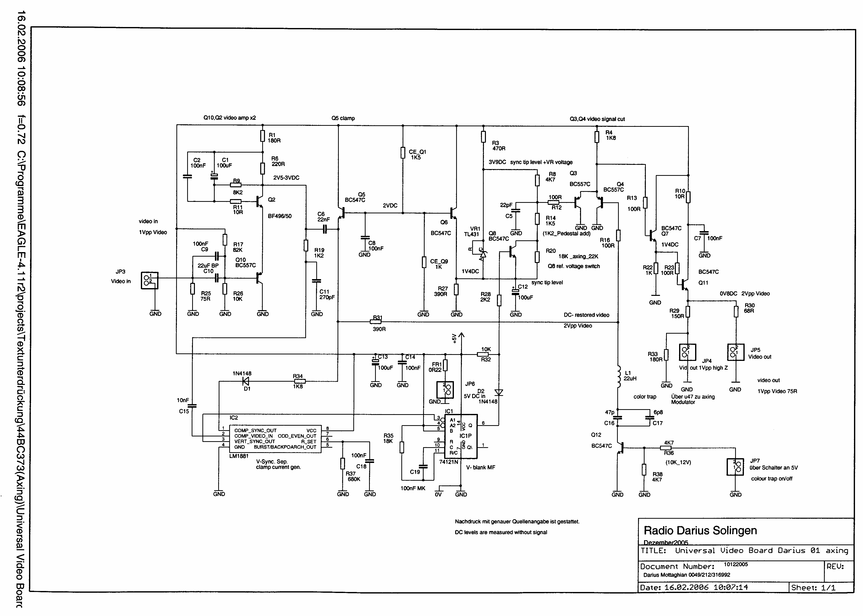
The complementary circuit technology enables the coupling of both branches of the differential amplifier without the separate "Power Supply". A complementary differential amplifier is used for example when UVB ; Q10 and Q2 form its complementary differential amplifier branches, here in the asymmetrical design. The interconnection
be the anode and katodengekoppelten differential amplifier,
disappeared following the Gleichtaktverkopplung *
the separate "power sources", the sun, would be for both differential amplifier alone, are needed.
measurements on the circuit:
large signal
The figure I have registered with the digital multimeter (R = 10MΩ) measured dc voltages.

For maximum headroom, should it ever fall ≈ ¼ of the operating voltage of the transistors and resistors work. Accordingly, the divider resistors R4, R12 and R19 are sized. If R11 is short, lying on the collector of Q1 and the collector of Q2 20VDC 16VDC. The current gain of the transistors is B ≈ 500th
small signal
rEasym measurement of the input resistance of the circuit:
5:00 input signal 1KHz sine of-20dBu, 200mVpp corresponding to X1, X2 it short. Output voltage at X3, X4 measure. -14dBu, so 400mVpp debug via resistance at X1, resistance value for the same output voltage. The
be considered resistance value is 56KΩ. The same value is obtained for X2 at short circuit of X1.
NAV
rEasym = R3 II R9 II hfe x (R10 + 1 / s)
rEasym = 1MW II 100ppm II 500 x (200Ω + 15Ω)
rEasym = 1MW II 100ppm II 108KΩ = 49KΩ
The input resistance rEasym is ≈ 50KΩ .
Tip:
The input capacity is at its lowest when the two differential amplifier operate asymmetrically and is used in phase to the input output lying. In plain English, if X1 is input to X2 and X3 and X4 grounded used as an output. The signal emitter follower → Basic Amplifier (with local negative feedback) → emitter follower provides a very fast broadband and amplifier topology. It is therefore used in a complementary form of the Universal video board.
measurement of the output resistance of the circuit
6.oo output resistor between the emitters of Q3 and Q4 ree:
sine of 1kHz-46dBu to feed at the entrance. Load resistor at the output X3-X4 Sun debug that the level of breaks in half. The ausgeürpfte ree resistance is 30Ω.
The measurement is whether it is symmetrical thus carried out between the two outputs X3-X4 or asymmetric, an output to GND, the other output to the load.
calculation of the output resistance according 4:01
6:01 The slope s = Ie / Ie = UT
6VDC/2K2Ω = 2.7 mA emitter current
UT = 40mV voltage temperature silicon
s = 2.7 mA/40mV = 68mA / V
1 / s = 15Ω
6:02 ree = 2 / s = 30Ω
7:00 output resistance rkm to X3 when X4 is open and vice versa:
sine of 1kHz-20dBu input on feed. Load resistance Sun debug output on X3, that the level of breaks in half. It is an open X4. The value to be considered rkm is 560Ω. The same value results in the measurement of X4 with open X3.
calculation analogous to 4:05
Rages R1 = R2 = II 1K1Ω
Rkges R16 = R15 II II II R17 R18 = 1K1Ω
rkm = (Rages + 1 / s) II Rkges
rkm = (1K1Ω + 15Ω) II 1K1Ω
rkm = 554Ω
8:00 The following measurement shows that the output can float:
of 1KHz sine-6dBu (equivalent to 1 Vpp) to the output X3 celling. Inputs are shorted it. The signal which is fed to X3 comes in, X4 out. The same vice versa so signal on X4 from X3 comes out.
This is also true for applications with FET's and tubes. Especially when
push-pull driver with Tubes get the start in Blog declared properties that offer a significant technical advance over the 'prior art'.
To be continued ...

(23.08.2009) Reactions to this blog in forums, it may be laughed:
"The ELKO 'attempt to Forum discussion on the blog. Warning, this thread now consists of several Pages, which you can choose above right. Meanwhile, I have the impression that people are overburdened with the subject. Reason: differential amplifier on the search for a basic link to the topic, I came across this page (release 16.07.09) . There, they claimed, the difference amplifier is the basic circuit of the operational amplifier and the picture shows a push-pull amplifier. This then had to serve for the explanation of the differential amplifier. I tried something decent in the associated forum to address . Obviously not because you understand it, but my "world view not to get shaken", one has in the second Tests (call 22:07:09) nevertheless already struggled through the LTP. To my question whether the difference between difference and is known push-pull amplifier, was to me the answer. Consequently, is it possible not to provide push-pull CMRR for the amplifier. 5th Page in the thread logically only if the declaration on the common-mode rejection from the 3.Versuch (release 18.08.2009) reads. By the way: Since the push-pull amplifier differential and total gain (ideally) have the same amount, the ratio 'CMRR' is then equal to one. Whether this criticism, the artist encourages thinking from self-proclaimed "electronic compendium 'to order? After five pages (!) Debate and hostility in the forum, I have little hope.
* www. ebmule de. Herrlich, the reaction of the Ing ... the breaks on the Gleichtaktverkopplung understanding between the differential amplifier tube stages. http://www.ebmule.de/printthread.php?tid=1147
quote from 07/27/2009 20:43 :"... your insane Gleichtaktverkopplung between the tubes exists only in your head. is the purely technical connection between the tubes cold. They can be easily ground to alternating voltage, without even one iota of change in the function. ... " End of quote.
but he had, see Start Block bottom, the Anordnung für sich verbuchen wool. Der Thread steht in der Fassung vom 06.08.2009 as pdf copy zur Verfügung und kann auf Anfrage privat zugesandt were.
Letzte Bearbeitung am 03.September 2009 (Text ebmule hi-portal)
Der folgende blog deals Schutzmaßnahmen in der Endstufe.

This work is licensed under a Creative Commons
Attribution-Noncommercial-No Derivative Works 2.0 Germany License .
0 comments:
Post a Comment